
ファイル:Solid state electronic band structure.svg

元のファイル (SVG ファイル、388 × 177 ピクセル、ファイルサイズ: 29キロバイト)
ウィキメディア・コモンズのファイルページにある説明を、以下に表示します。
|
概要
| 解説 |
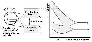
English: Diagram illustrating how electronic band structure of a solid comes about by the hypothetical example of a large number of carbon atoms coming together to form a diamond crystal lattice. The graph (right) shows the energy levels of the atoms as a function of the spacing between atoms. When the atoms are far apart (right side of graph) each atom has valence atomic orbitals p and s which have the same energy. However when the atoms come closer together their orbitals begin to overlap. The Pauli Exclusion Principle dictates that no two atoms in a molecule can have electrons with the same quantum numbers, so each atomic orbital splits into N molecular orbitals each with a different energy, where N is the number of atoms in the crystal. Since N is such a large number (~1022) adjacent orbitals are extremely close together in energy (~10-22 eV) so the orbitals can be considered a continuous energy band. a is the atomic spacing (lattice constant) found in an actual crystal lattice of carbon atoms (diamond lattice) so the band structure at that spacing is the one found in diamond. At that spacing the orbitals form two bands, called the valence band and conduction band, with an energy gap of 5.5 electron volts (eV) between them. The valence electrons fill the lower band. Electrons in this band are not mobile; while electrons in the higher conduction band can travel through the crystal from atom to atom, and thus serve as charge carriers to conduct electricity. Since the 5.5 eV band gap is much larger than the thermal energy of most electrons in the crystal, very few electrons acquire the energy to jump the gap and become conduction electrons. This is why diamond is an electrical insulator. |
| 日付 | |
| 原典 | 投稿者自身による著作物 |
| 作者 | Chetvorno |
| SVG 開発 |
ライセンス
| このファイルはクリエイティブ・コモンズ CC0 1.0 全世界 パブリック・ドメイン提供のもとで利用可能にされています。 | |
| ある作品に本コモンズ証を関連づけた者は、その作品について世界全地域において著作権法上認められる、その者が持つすべての権利(その作品に関する権利や隣接する権利を含む。)を、法令上認められる最大限の範囲で放棄して、パブリック・ドメインに提供しています。
この作品は、たとえ営利目的であっても、許可を得ずに複製、改変・翻案、配布、上演・演奏することが出来ます。 |
ファイルの履歴
過去の版のファイルを表示するには、その版の日時をクリックしてください。
| 日付と時刻 | サムネイル | 寸法 | 利用者 | コメント | |
|---|---|---|---|---|---|
| 現在の版 | 2017年5月9日 (火) 02:58 | | 388 × 177 (29キロバイト) | Chetvorno | Replaced invalid Inkscape SVG version with "plain SVG" version which passes validation |
| 2017年3月10日 (金) 20:06 |  | 388 × 177 (35キロバイト) | Chetvorno | User created page with UploadWizard |
ファイルの使用状況
以下のページがこのファイルを使用しています:
グローバルなファイル使用状況
以下に挙げる他のウィキがこの画像を使っています:
- bn.wikipedia.org での使用状況
- en.wikipedia.org での使用状況
- fa.wikipedia.org での使用状況
- fi.wikipedia.org での使用状況
- fr.wikipedia.org での使用状況
- ml.wikipedia.org での使用状況
- nl.wikipedia.org での使用状況
- ro.wikipedia.org での使用状況