
ファイル:NE555 Bloc Diagram.svg

元のファイル (SVG ファイル、723 × 524 ピクセル、ファイルサイズ: 32キロバイト)
ウィキメディア・コモンズのファイルページにある説明を、以下に表示します。
|
概要
| 解説 |
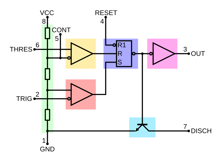
English: The NE555 contains 24 bipolar transistors, two diodes and 15 resistors that form six functional blocks:
Between the supply voltage VCC (+) and the ground GND (-) is a voltage divider consisting of three identical resistors which, when connected not from the outside, the two reference voltages ¹ / 3 VCC and ² / 3 VCC supplies. The latter is at the terminal pin Control Voltage available. The block diagram and schematic that area is highlighted in green. Two comparators are each connected to one of the reference voltages, while the other two inputs of which are fed directly to the terminals of trigger or threshold. The block diagram in yellow and orange. A flip-flop, deposited in the color purple, stores the state of the timer and is controlled by the two comparators. Via the reset terminal overrides the other two inputs, the flip-flop (and therefore the entire timer device) be reset at any time. At the output of flip-flop followed by an output stage with totem-pole output that can be loaded at the port output with up to 200 mA. Shown in the color pink. Parallel to the output stage of a transistor is connected, the collector is located on the discharge port. The transistor in the circuit diagram is a light blue background, always energized when the output is low level.Deutsch: Der NE555 enthält 24 Bipolartransistoren, zwei Dioden und 15 Widerstände, die zusammen sechs Funktionsblöcke bilden:
|
| 日付 | |
| 原典 | 投稿者自身による著作物 |
| 作者 | BlanchardJ |
| その他のバージョン |
  |
ライセンス
| この著作物の著作権者である私は、この著作物における権利を放棄しパブリックドメインとします。これは全世界で適用されます。 一部の国では、これが法的に可能ではない場合があります。その場合は、次のように宣言します。 私は、あらゆる人に対して、法により必要とされている条件を除き、如何なる条件も課すことなく、あらゆる目的のためにこの著作物を使用する権利を与えます。 |
ファイルの履歴
過去の版のファイルを表示するには、その版の日時をクリックしてください。
| 日付と時刻 | サムネイル | 寸法 | 利用者 | コメント | |
|---|---|---|---|---|---|
| 現在の版 | 2012年1月16日 (月) 19:54 | | 723 × 524 (32キロバイト) | Wdwd | Colored function blocks (for circiut diagram) correct transistor symbol (without a circle, because it's inside the chip) |
| 2009年6月7日 (日) 23:27 |  | 723 × 524 (40キロバイト) | Brighterorange | remove spurious red dot | |
| 2007年9月23日 (日) 20:22 |  | 723 × 524 (40キロバイト) | BlanchardJ | {{Information |Description=Bloc diagram of a 555 timer IC |Source=self-made |Date=September 23 2007 |Author=BlanchardJ |Permission= |other_versions= }} {{Created with Inkscape}} {{ElCompLib}} Category:555 timer IC |
ファイルの使用状況
以下のページがこのファイルを使用しています:
グローバルなファイル使用状況
以下に挙げる他のウィキがこの画像を使っています:
- ar.wikipedia.org での使用状況
- beta.wikiversity.org での使用状況
- ca.wikipedia.org での使用状況
- cs.wikipedia.org での使用状況
- cs.wikibooks.org での使用状況
- de.wikipedia.org での使用状況
- en.wikipedia.org での使用状況
- es.wikipedia.org での使用状況
- et.wikipedia.org での使用状況
- fa.wikipedia.org での使用状況
- fi.wikipedia.org での使用状況
- fr.wikipedia.org での使用状況
- fr.wikiversity.org での使用状況
- he.wikipedia.org での使用状況
- hi.wikipedia.org での使用状況
- hu.wikipedia.org での使用状況
- id.wikipedia.org での使用状況
- it.wikipedia.org での使用状況
- lt.wikipedia.org での使用状況
- no.wikipedia.org での使用状況
- pl.wikipedia.org での使用状況
- pt.wikipedia.org での使用状況
- ru.wikipedia.org での使用状況
- uk.wikipedia.org での使用状況
- vi.wikibooks.org での使用状況
- zh.wikipedia.org での使用状況